Divide-and-Conquer Physical Design Cycle Physical. Due to the advent of VLSI.
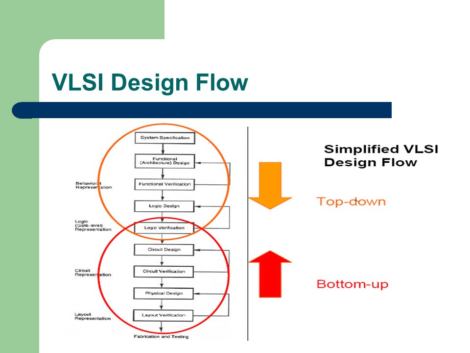
Vlsi Design Flow
Chart and Diagram Slides for PowerPoint - Beautifully designed chart and diagram s for PowerPoint with visually stunning graphics and animation effects.
. Full syllabus notes lecture questions for Introduction to Digital VLSI Design Flow - PPT Engg Sem. 0 found this document useful 0 votes 100 views 23 pages. Revised June 10 2002.
Clock Cycle for Data Management- VLSI Design. Speed 1 10 nSec 100 MHz Latency 3 clock cycles tp230 register t p 05 create_clock clk -period 10 pipeline_design -stages 3 optimize_registers tp95 tp5 tp87. Shall consider interconnections in early design stages.
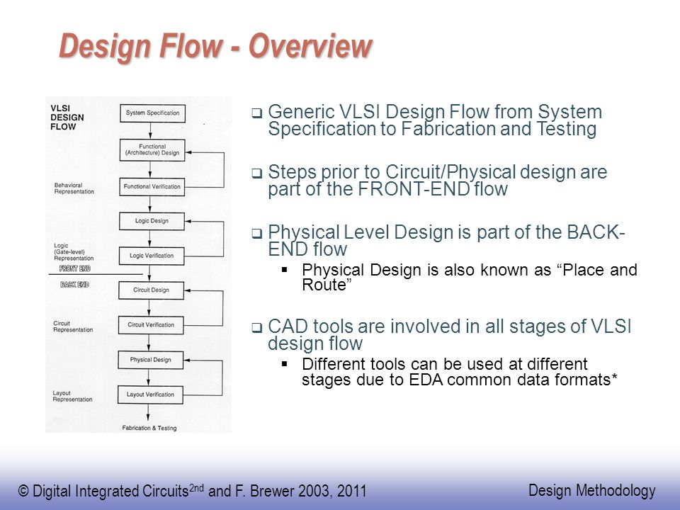
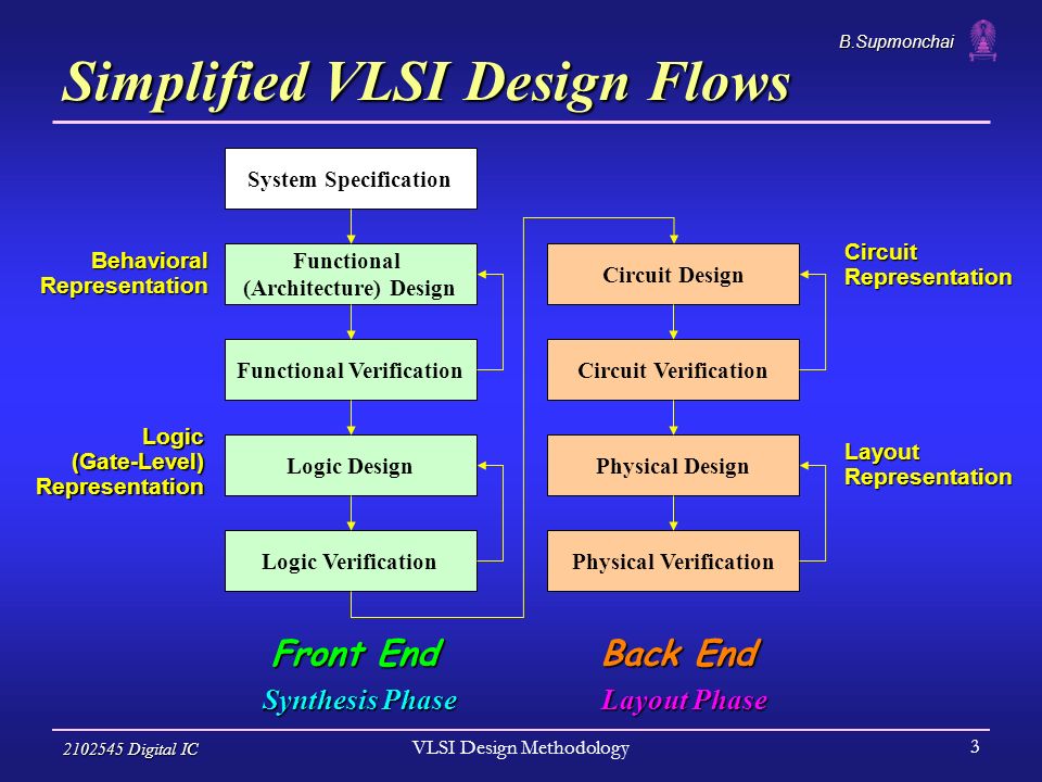
VLSI design Flow 1System Specification. The available tools require enormous human intervention to implement the complete system Conclusion The demand for low power VLSI digital circuits in the growing area of portable communications and computing systems will continue to increase in the future. Istics of a digital design.
Design and Simulation of VLSI Processor Design and Simulation of the VHDL. ELEC 5770-0016770-001 Fall 2010 VLSI Design Low Power VLSI Design - Larsson Introduction to Advanced. On rising output charge Q CVDD is required On falling output charge is dumped to GND This repeats Tfsw times over an interval of T Dynamic Power Cont.
Our new CrystalGraphics Chart and Diagram Slides for PowerPoint is a collection of over 1000 impressively designed data-driven chart and editable diagram s guaranteed to impress any audience. Design productivity is usually very low. Unit 1 14 Y-W.
VLSI Design Methodologies Full Custom Design Semi Custom Design Gate Array Design Standard Cell Design FPGA Based Design CPLD Based Design Hardwired Control PLA Based Control HDL Based Design Methodology RT-Level Synthesis IP Cores SOCs DSPs MEMs VLSI Design Cycle 19 System Specification Circuit Design Architectural Design Physical Design Functional. The first step of any design process is to set the specifications of the system. VLSI Design - Digital System.
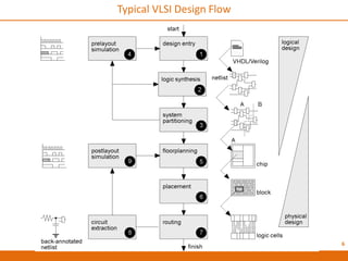
The digital design is still a bottleneck. Download as PPT PDF TXT or read online from Scribd. Partition Clustering Floorplan Placement clk clk clk a a a Pin Assignment Global Routing Global Routing Detailed Routing Methodology.
This compares the power consumption and delay of radix 2 and modified radix 4 Booth multipliers. The VLSI design cycle starts with a formal specification of a VLSI chip follows a series of steps and eventually produces a packaged chip. Typically 10 to 20 transistors per day per designer.
Area speed power dissipation noise design time testability etc. Cessed per clock cycle bits per second and processed data output clock cycle ential elements clock period the timing it. Nov 16 ELEC5770-0016770-001 Guest Lecture CMOS Gate Power V Ground.
Latency 1 clock cycle Max. Save Save 02 Introduction to VLSI and ASIC Designppt For Later. Outputs C7-C11 from the.
Sequencing Overhead Use flip-flops to delay fast tokens so they move through exactly one stage each cycle. Harris CMOS VLSI Design Third. VLSI Design of Low Power Booth Multiplier Nishat Bano Abstract-This paper proposes the design and implementation of Booth multiplier using VHDL.
Sequential Circuits 5CMOS VLSI DesignCMOS VLSI Design 4th Ed. VLSI began in the 1970s when complex semiconductor and communication technologies were being developed. In digital CMOS VLSI full-custom design is rarely used due to the high labor cost.
The electronics industry has achieved a consistent growth over two decades mostly to the advances in integration technologies and large-scale systems design ie. Chang Traditional VLSI. In this paper we detail circuit and analysis techniques used to complete this high-performance design.
Notes - Electronics and Communication Engineering ECE - Electronics and Communication Engineering ECE Plus excerises question with solution to help you revise complete syllabus Best notes free PDF download. Critical path in any design is the longe 1. The microprocessor is a VLSI device.
VLSI Design 2 Very-large-scale integration VLSI is the process of creating an integrated circuit IC by combining thousands of transistors into a single chip. Flag for inappropriate content. Interconnect not gate delay dominates circuit performance in deep submicron era.
Interconnects are determined in physical design. Inevitably adds some delay to the slow tokens Makes circuit slower than just the logic delay Called sequencing overhead Some people call this clocking overhead. The microprocessor is a VLSI device.
The number of applications based on. Experimental results demonstrate that the modified radix 4 Booth multiplier has 229 power reduction. Manuscript received March 15 2002.
Switch either 0 or 2. VLSI Design Flow VLSI very large scale integration lots of transistors integrated on a single chip Top Down Design digital mainly coded design ECE 411 Bottom Up Design cell performance Analogmixed signal ECE 410 VLSI Design Procedure System Specifications Logic Synthesis Chip Floorplanning Chip-level. SRAM Outline Memory Arrays SRAM Architecture SRAM Cell Decoders Column Circuitry Multiple Ports Serial Access Memories Memory Arrays Array Architecture 2n words of 2m bits each If n m fold by 2k into fewer rows of more columns Good regularity easy to design Very high density if good cells are used 12T SRAM Cell Basic building block.
Introduction to Low Power Design in VLSI Mtech ECE Presentation. Activity Factor Suppose the system clock frequency f Let fsw af where a activity factor If the signal is a clock a 1 If the signal switches once per cycle a ½ Dynamic gates. VLSI began in the 1970s when complex semiconductor and communication technologies were being developed.
Cost and life cycle of these. Exceptions to this include the design of high-volume products such as memory chips high-performance microprocessors and FPGA masters. Outputs C1-C6 from the Clock Controller.
Very-large-scale integration VLSI is the process of creating an integrated circuit IC by combining thousands of transistors into a single chip. Any two internal latchesflipflops. All IEU operations require a half cycle for execution and a half cycle for bypass allowing each ALU result to be used in the next cycle as a source for ALU or data cache addresses.
Inputs to the Clock Controller. Approach to system design cycle b workable transistors models. Low Power Design in VLSI Mtech ECE Presentation PPT.
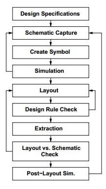
Conventional physical design cycle consists of 1 Partitioning Floorplanning Placement Routing Compaction Physical Design Physical Design Process Design Steps. Microsoft PowerPoint - Final Presentation Author.
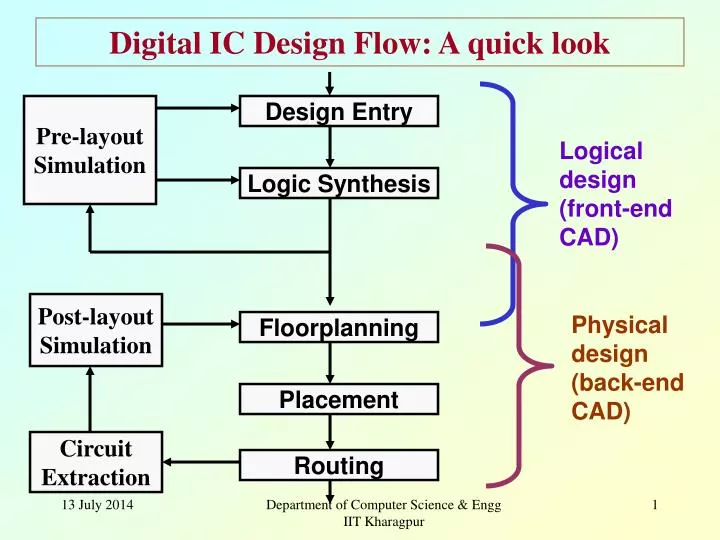
Ppt Digital Ic Design Flow A Quick Look Powerpoint Presentation Free Download Id 1733065
Ece 224a Cmos Vlsi Design Lab Ppt Video Online Download

Vlsi Design Flow

Vlsi Design Introduction Ppt Download
Vlsi Design Introduction Ppt Download

Vlsi Basics Vlsi Design Flow
Tutorial 3 Vlsi Design Methodology Boonchuay Supmonchai June 10th Ppt Download
Vlsi Design Digital System
0 comments
Post a Comment